![]() Our
works and applications
Our
works and applications
|
|
|
|
|
- One of starting applications of EBL was realization of submicrometer structures for investigation of plasma etching procedure of aluminium. - The fabrication of photomasks. Fabrication of photomasks was realized for many national or foreign partners. Examples (click to enlarge; request for full quality images send to address ivan.kostic@savba.sk or fully fill form):
- Fabrication of photomasks for development of custom-designed circuits GAC 1200 and GAC 4000 dedicated to exploitation in industry.
- Development of technology and fabrication of quartz photomasks for DUV (248-196nm) photolithography and resolution from 250 to 300 nm.
- Development of technology and realization of direct writing electron beam lithography on semiconductor substrate and superconducting thin films realized for many national or forein partners.
- Participation in design, construction, development and realization of new progressive method of forming microstructures in microsystem technology using direct electron beam lithography and plasmatic anisotropy etching – LIRIE (Lithography and Reactive Ion Etching) to exploitation for further development and fabrication of micro-electro-mechanical systems (MEMS) based on monocrystalline silicon. The LIRIE technology was completely developed and built-up in collaboration with IMA Institute University of Kassel, Germany.
- Development and realization of elements for detection and analysis of microelements in cosmos space and their in-situ analysis (cooperation with TU Vienna, Austria, MIDAS - Micro Imaging Dust Analysis System – main applicator - European Space Agency).
- Patent USA No. 6.136.160 from 24.10.2000, Process for Producing a Carbon Film on a Substrate. Authors: P. Hrkút, P. Hudek (Dept. of EBL), I. W. Rangelow (University of Kassel, Germany), H. Löschner (IMS GmbH, Wien, Austria). Subject of patent is design and realization of technological deposition sequence of carbon layers with determination of residual stress in layers also on the top of thin membranes and verification of mask properties of this layer aplicable like a STOP-layer and bombed of Si-membrane by He+ ions. Objectives of discovering are charakterization of physical, electric and mechanical properties of carbon layer with laminar – nanometrical structure.
- The mask fabrication for development and realization of integrated cantilevers for several unconventional types of Scanning Probe Microscope (SPM). Main applicator - University of Kassel, Germany.
- Development of technology for preparation of submicrometer structures in thin silicon membranes that can be used as an open-stencil mask for ion projection lithography or sensor technics.
- Realization of optical elements (random phase plate). Main applicator - Dept. of Atomic Physics, TU Budapest, Hungary.
- Development of technology for preparation of STW and SAW elements with submicrometer details (0,4μm) for frequency band to 2,5GHz. Main applicator M-tron Industries, Inc., Yankton, South Dakota, USA.
- Development of technology of microelectromagnetical matrix for investigation of nanoparticle self-organization. Main applicator Institute of Physics Slovak Academy of Sciences.
- Development of NINI – design system & data preparation and structure drawing (author Ing. Peter Hudek) for input data preparation to electron lithographic system ZBA10/1 with correction of proximity and thermal effects before exposure of pattern in electron beam resist. - Participation on development of lithographic module ELITHA 32 (PMS GmbH, Herver, Germany) using innovated version of NINI (Dr. Peter Hudek and RNDr. Miroslav Belov). This module is commercially offered for sales. Research & Development, design, construction, realization and fabrication - Simulation of interaction of electron beam with system „resist-substrate“. - Development of methods of proximity effect correction in electron beam lithography.
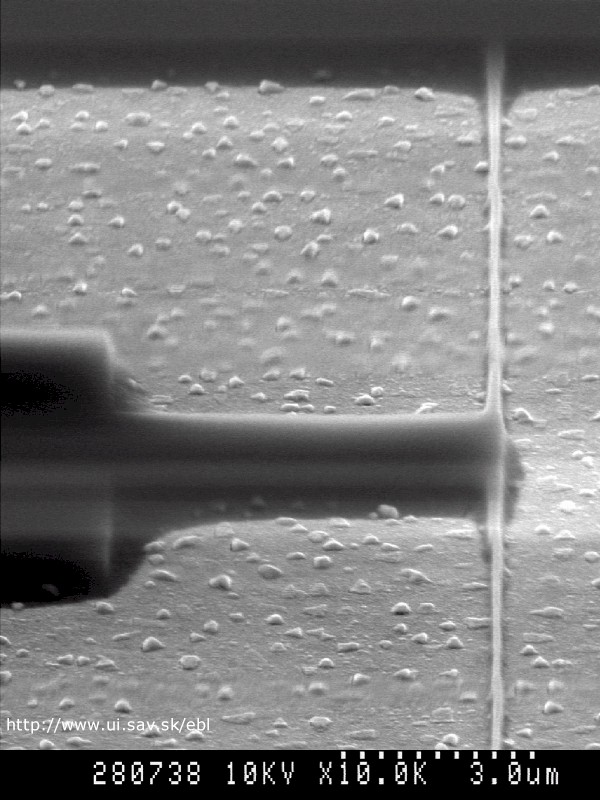
- Direct multilayer electron beam lithography of submicrometer and nanometer structures on semiconductor substrates. - Preparation of micro lithographic pattern for photolithography and deep-UV lithography by electron beam lithography. Minimal size of borosillicates structures is 300-400nm and Minimal size of silicon structures is 200-300nm.
- Investigation of new resist materials and their optimalization for processes in electron beam lithography.
- Investigation of new methods of thin-film structures preparation for sensors and microsystems applications.
- Substrate surface modification for nanotechnological applications, e.g. for preparing of organized quasi-2-dimensional layers of nanoelements.
- Thin metal and dielectrical layers deposition by d.c. or r.f. sputtering with high homogenity (around 5%) to substrate with maximum size 17x17 cm with previous clearance by electrical discharge and indirect heating of substrate. - Deposition of multicomposition metal layers – laminar structures by electrom beam evaporation in one vacuum cycle. - Preparation of structures by reaction ion etching. - Preparation and deposition of polyimide thin layers for insulative applications, passivation applications and sensors. |
|
|